|
 |
| The light emitted by a scintillation material
must be detected using some kind of sensitive light detection device. Basically, there are
two options :
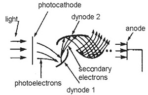
Light (photons) is converted into photoelectrons by absorption in a thin photocathode layer inside a (glass) vacuum tube. Most often a photocathode is semi-transparent and usually consist of a thin layer of evaporated Cs, Sb, and K atoms or a mixture of these. Each photoelectron is pulled by an electric field towards a dynode and subsequentially amplified. In a 12 stage PMT, the net amplification is of the order of 10 6. Each scintillation pulse produces a charge pulse at the anode of the PMT. The process is illustrated below. |
||||||||||||||
 |
||||||||||||||
Besides in the above described pulse mode, PMTs can also be operated in current mode in which case the anode current is a measure for the integral radiation intensity absorbed in the scintillator. This method is only used at high count rates. In a photodiode, the scintillation photons produce electron-hole pairs that are collected at respectively the anode and the cathode of the diode. Most frequently, reverse biased PIN photodiodes are used having a low capacitance and leakage current. In the following section, the above detection mechanisms are discussed in more detail. |
||||||||||||||
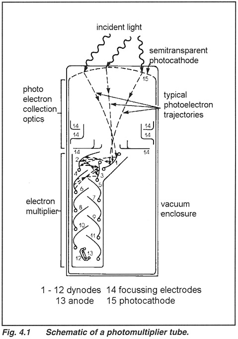
| Photomultiplier Tubes The energy resolution, coincident resolving time and stability of a scintillation detector depend to a great extent upon the type of photomultiplier tube. The selection of a proper type is fundamental to a good detector design . The light conversion efficiency of a photomultiplier cathode is a function of the wavelength; the Quantum Efficiency (Q.E.) is defined as the chance that one photon produces one photoelectron. In the amplification process, one photoelectron produces per dynode step about 3 - 4 secondary electrons. With a 12 stage PMT, a typical gain in the order of 10 6 can be obtained. Fig. 4.1 shows a schematic of a PMT. It should be noted that PMTs are sensitive to magnetic fields; a m-metal shield provides adequate protection from the earth magnetic field. For operation in high magnetic fields, special PMTs are available. |
||||||||||||||
 |
||||||||||||||
There exist a number of PMT dynode structures, each with their typical characteristics. Important PMT parameters are :
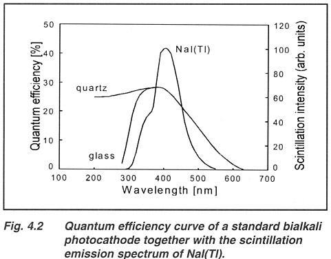
Gain, stability and dark current depend on the used dynode materials and are a function of temperature. Pulse rise time depends on the dynode structure. For fast timing applications, so called "linear focused" PMTs are advised. A very important factor is the sensitivity as a function of the position on the PMT entrance window. A large variation can cause a degradation of the energy resolution of a scintillation detector. This variation can be caused by a change in quantum efficiency of the photocathode or a non-uniform photoelectron collection efficiency from the cathode onto the first dynode. The above effects can be important for both small and large diameter PMTs. From Table 3.1 it is clear that each type of scintillator has a different emission spectrum. It is important for a good performance that the emission spectrum of a scintillator is well matched to the quantum efficiency curve (for definition see above) of the PMT. To detect the fast scintillation component of BaF 2 for example, it is necessary to use a PMT with quartz window since glass absorbs all light below 280 nm. Fig. 4.2 shows the quantum efficiency (Q.E.) of a standard PMT with a bialkali photocathode. The emission spectrum of the most common scintillator NaI(Tl) is shown too. It can be seen that the overlap is very good. For other scintillation materials such as BGO, the match is less ideal. The gain of a PMT is temperature sensitive. The variation in gain, which depends on the photocathode and dynode material, amounts to typically a few tenths of a percent per oC. Due to their dynode stages, PMTs are usually quite bulky devices although some short versions and miniature types have been developed. Care must be taken when PMTs are used inside magnetic fields. Although there are PMT types that have a high magnetic field immunity, this effect remains a problem. The material of a PMT is usually glass. Glass has an intrinsic amount of 40K which contributes to the radiological background of the scintillation detector. 40K emits as well 1460 keV gamma rays as beta particles. The face-plate of the PMT can be constructed of special low-K glass. Furthermore, this background can be limited by using light guides absorbing the b-particles and creating a distance between the crystal and the PMT. The above techniques are used in so-called "low background" scintillation detectors. Below we would like to summarize the advantages and disadvantages of PMTs in conjunction with scintillation crystals. For more information regarding PMTs we refer to the PMT manufacturer's literature. Photomultiplier Tubes
|
||||||||||||||
 |
||||||||||||||
| BACK TO TOP | ||||||||||||||
|
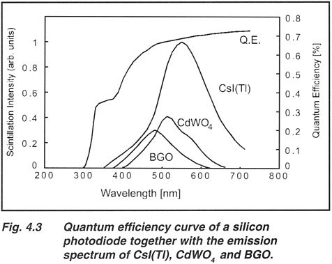
An alternative way to detect the scintillation light from a crystal is the use of a silicon photodiode. This is a semiconductor device which consists of a thin layer of silicon in which the light is absorbed after which free charge carriers (electrons and holes) are created. Electron and holes are collected at the anode and cathode of the diode. Most frequently used are PIN diodes operated in reverse bias mode. When these photodiodes (usually of the PIN type) are optically coupled to a scintillation crystal, each scintillation light pulse will generate a small charge pulse in the diode which can be measured with a charge sensitive preamplifier. Alternatively, the current produced in the diode can be measured. The quantum efficiency of silicon photodiodes is typically 70 % between 500 and 900 nm but decreases rapidly below 500 nm as shown in Fig. 4.3. It is clear that the highest signals can be expected from scintillation crystals that have an intense emission above 500 nm. CsI(Tl) crystals, characterized by a large scintillation intensity with a maximum at 550 nm, are therefore well suited to couple to photodiodes. In contrary to photomultiplier tubes, photodiodes do not require a high voltage (HV) power supply but only a bias voltage of about 30 V. Photodiodes are thin, rugged and insensitive to magnetic fields. Furthermore, the output signal from a crystal/photodiode detector is very stable due to the absence of drift of the diode gain since no charge amplification takes place in the device itself. Photodiodes are thin (several mm) which can be advantageous. Due to the small signal generated by the photodiode, it is necessary to employ a high quality charge preamplifier in order to keep the noise level as low as possible. Noise is an intrinsic problem to standard photodiodes. In silicon PIN photodiodes, the created number of primary electron-hole pairs (e-h pairs) is not increased by amplification. The PIN photodiode is a unity gain device. The thickness of the silicon used is typically 200 - 500 mm. Coupled to a conventional (low noise) charge sensitive preamplifier, the substantial capacitance of the device (40 - 50 pF/cm2 for 200 and 300 mm wafer devices) is mainly responsible for the noise which determines for a large part the energy resolution of the detector. Also the dark current of PIN photodiodes (1 - 3 nA/cm2 at full depletion) may contribute significantly to the noise, especially at larger shaping times. The dark current increases as well with increasing surface area as with increasing temperature. |
||||||||||||||
 |
||||||||||||||
Some typical noise numbers are:
|
||||||||||||||
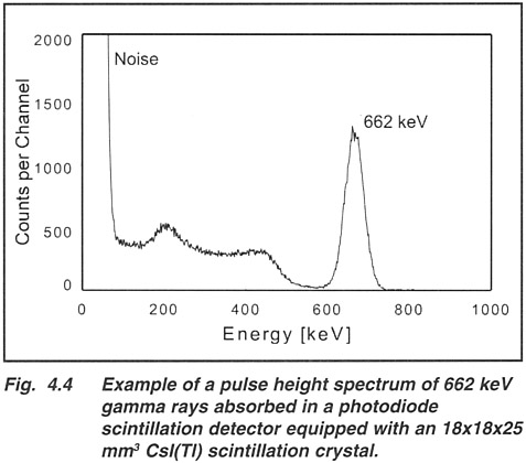
As long as there is enough light per event available, every scintillation event can be detected using photodiodes. However, due to the intrinsic noise there is a lower limit on the energy of the radiation that can be detected. For a small (1 cm3) CsI(Tl) cube coupled to a 10 x 10 mm2 photodiode the best lower energy limit reported amounts to 37 keV. From the above noise numbers and the electron-hole pair yield of the scintillator/ photodiode combination, the noise contribution to the energy resolution can be calculated. Fig. 4.4 shows a pulse height spectrum measured with a photodiode scintillation detector. At increasing temperatures, the dark current of the photodiode increases. This limits the use of scintillation photodiode detectors to temperatures below 50 oC. On the previous page we summarize the advantages and disadvantages of photodiode scintillation detectors in conjunction with scintillation crystals for pulse counting. Photodiodes can also be used in DC mode to read out a scintillation crystal. Capacitance and leakage current are less important then since the diode is used unbiased. This mode of operation is used for applications where radiation intensities are high and close packing of arrays of scintillation crystals is required such as in medical CT scanners. The low level noise limit can be overcome by using so-called "Avalanche Photodiodes", APDs. These devices can also detect X-rays of lower energy by using internal amplification. However, an external voltage of at least several hundred Volts is required and the amplification is a strong function of temperature (gain stability). Also, the leakage current of APDs at room temperature is relatively high. APDs are currently available in approximately 1 cm diameter size maximum. APD signals are much faster than signals from PIN diodes and are mostly used for fast timing with small scintillation crystals. Scintillator Photodiode Detectors
|
||||||||||||||
 |
||||||||||||||
| BACK TO TOP | ||||||||||||||