|
In this chapter some general aspects are mentioned regarding detector construction which may help you choosing the right detector for your application. |
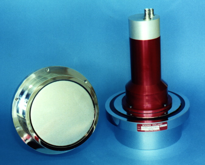
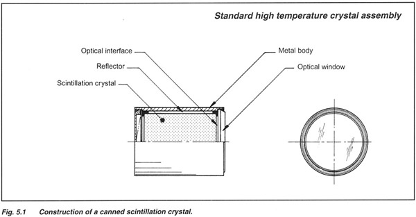
Scintillation crystals without photomultiplier tubes A scintillation crystal can be supplied to fit user specifications. The scintillation crystal is usually supplied in a hermetically sealed metal container to protect the crystal from hydration (NaI(Tl)) or to protect the crystal from other environmental influences. In case of nonhygroscopic crystals this requirement is less stringent. Because of statistics, it is always desirable to detect as much light as possible from a scintillation event in the light detection device. For this purpose, the scintillation crystal is covered on all sides, except the read-out side, with reflective material. This can be e.g. white reflective paper, teflon or reflective powder such as MgO or Al2O3. The surfaces in contact with the reflector can be optically polished or ground. The scintillation light is transmitted through a glass or quartz window to be optically coupled to the PMT entrance window. Depending on the shape of the scintillation crystal, a certain surface treatment is required to obtain a large light output and a good uniformity. Both are important to achieve a good energy resolution. The optimization of scintillation crystal surfaces is based on experience with the material and not always obvious. In case of axial or transverse wells in the crystal (see section 7), different types of surface treatments are required to ensure a homogeneous response. In general it is advisable to choose the diameter of the scintillator slightly smaller than the diameter of the PMT since the outer area of a PMT is often less sensitive that the center. Optical coupling to the PMT can be achieved by using optical grease or a special optically transparent glue. In Fig. 5.1 the general construction of a canned scintillation crystal is shown. Flexible optical coupling allows for different expansion coefficients between materials. |
 |
|||
| BACK TO TOP | |||
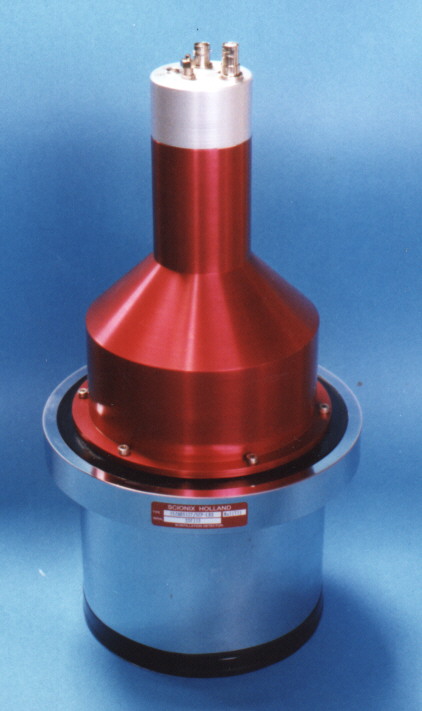
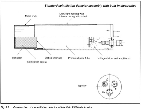
Scintillation crystals with photomultiplier tubes The most frequently used scintillation detector consists of a scintillation material integrally coupled to a PMT. The entire assembly is mounted in a metal housing with m-metal shielding against the influence of magnetic fields. For conditions where strong fields are expected, this shield can be increased in thickness for additional protection. Standard scintillation detectors read out with PMTs can be provided with either an external so called "plug-on" Voltage Divider (VD) for the PMT or with a built-in one. In the first case, the detector itself ends in a 12, 14, 20 or 21 pins connector that should be plugged into the socket of the VD. This allows quick exchange of detectors and electronics but it makes the detector considerably longer (about 5 cm). For more details regarding detector electronics we refer to section 8. For low background applications, a built-in VD is always advised since this avoids the use of connector materials which are often a source of background. Fig. 5.2 shows a detector with integrally connected PMT and built-in voltage divider / emitter follower. |
 |
|||
| BACK TO TOP | |||
|
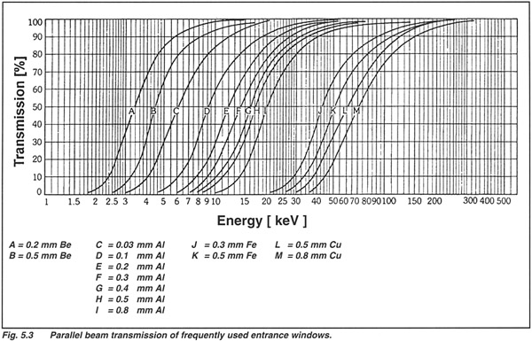
The density and thickness of the detector entrance window determine the transmission of the radiation. For high energy gamma-rays say > 300 keV, the absorption of a mm or so entrance window can be neglected and the choice for a window is dictated by practical considerations. For lower energy X-rays this choice is more critical. In Fig. 5.3 the transmission of a range of standard detector windows is presented from which you can determine the optimum window for your application. The thinnest Aluminum window normally used has a thickness of 25 -30 mm. This window can be used down to 10 keV X-ray energy. Below this energy, 0.2 or 0.3 mm thick Beryllium is required. The advantage of a Be window above a thin aluminum one is that is it less fragile. For the detection of low energy electrons (beta particles), a thin aluminized (light tight) mylar window is used. Mylar windows however can only be applied for nonhygroscopic scintillation materials (see section 3). Standard thickness is 25 or 100 mm. |
For the detection of alpha particles or heavy ions, a windowless detector (used in absolute dark, e.g. a vacuum vessel) or a very thin aluminized mylar window is used (typical thickness 2 mm). Some crystals are suitable to coat with several hundreds of nm evaporated aluminum for the detection of very low energy beta particles (e.g. from Tritium). |
 |
|||
| BACK TO TOP | |||
Crystal dimensions and housing materials As discussed in section 2.1, the surface area (solid angle) and the thickness of a scintillation crystal determine its detection efficiency. Normally, a scintillation crystal is read out with a PMT or a photodiode in dimension equal to one of its sides. However it is possible to use light guides or to taper a crystal without much loss of performance. This can save space and cost, especially when resolution is not of importance. The maximum size of a scintillation crystal varies very much between different materials. NaI(Tl) crystals can be manufactured up to around 0.5 m in diameter whereas e.g. the limit for good quality BGO crystals is around 15 cm. This has to do with crystal growing physics related to the physical properties of the material. The limit for Ce doped crystals like YAP:Ce is even smaller, 5 cm in diameter. Sometimes it is easier and less expensive to construct a large detector surface area by combining smaller detectors. We always advise to consult us for the optimum detector configuration for your application. Detectors can be supplied with cylindrical housings made of e.g. plastics (only non-hygroscopic crystals), aluminum, (chrome plated) steel, stainless steel or copper. More complicated geometries are possible but add to cost. Aluminum has excellent radiation transmission properties but is relatively soft and can corrode, even when anodized. For aggressive or rough environments (shocks), stainless steel is advised. Copper is useful for low background applications (see section 5.7). All detectors can be provided with customer defined mounting flanges or other means to support the instrument. |
| BACK TO TOP |
|
The light yield of a scintillation material and the gain of a PMT is a function of temperature. As discussed in section 2, it is possible to calibrate a scintillation detector on a light pulse emitted by e.g. a stabilized LED or by the light emitted by a radioactive pulser. This can be :
The advantage of method 1 is that one calibrates on the true response of the primary crystal. However, many gamma sources have more than one line and Compton background adds to the spectrum. The advantages of alpha sources is the absence of Compton background and their high energy (usually around 5 MeV) which implies narrow lines. The disadvantage is that the temperature response of many scintillation crystals is different for gammas and alphas. The optimum choice depends on the energy of interest and on the temperature region in which the detector should be stabilized. |
| BACK TO TOP |
|
The advantages and limitations of photodiode detectors were already discussed in detail in section 4. In general, the required size of the scintillation crystal determines the possibility to use this readout technique. Small crystals perform best with good energy resolution and noise levels around 50 keV or slightly less. For medical applications these devices are well suited for measurement of 140 keV gamma-rays in which case the CsI(Tl) scintillation crystal is chosen with 15 x 15 or 10 x10 mm surface area. Photodiode detectors are also widely used for heavy ion detection in combination with thin Si detectors for E / DE measurements applied to particle identification. Compact size, good energy resolution and immunity to magnetic fields are pros. A totally different application is the measurement of high intensity X-ray beams. In this case, the photodiode is used in DC current mode (no pulse height discrimination). Low afterglow scintillation crystals like CdWO4 are used in arrays coupled to photodiodes. Advantages are the good signal reproducibility, the absence of gain drift and the compact size. Examples of photodiode detectors are shown in section 7. |
| BACK TO TOP |
|
The term low background in itself needs to be specified in detail. A proper definition is the number of counts within a certain energy window with a well-defined shielding around the instrument (Pb, Fe and Cu). Sources of background from within the detector are the photomultiplier tube, the detector housing and the crystal. The main contributing nuclides are 40K (mainly from the PMT glass) and U and Th which are present in small quantities in the housing and window materials. Special PMTs can be selected with a ultra-low K content and all other materials can be pretested prior to assembly. Plastics should be avoided because these often contain K. Aluminum has a larger U and Th content than steel so for low background applications, steel housings are the best choice. In low background detectors special precautions are taken to reduce the internal background. Between PMT and crystal quartz or undoped NaI light guides are used to absorb the beta radiation from 40K and to increase the distance between the PMT and the scintillation crystal. The scintillation crystal is a source of internal contamination too. Standard NaI(Tl) crystals have a low background since their 40K content is less than 1 ppm. However, BGO crystals have an internal background that can be considerable and is approx 7 c/s/cc total (0 - 3 MeV). This background is caused by traces of 206Pb that are transmuted by cosmic radiation into 207Bi, resulting in gamma lines at 570, 1060, 1630 (sum peak) and 2400 keV. All BGO has this property. BaF2 crystals have an intrinsic background of Radium causing a set of alpha lines with a typical count rate of 0.2 c/s/cc. The best scintillation crystal for low background applications is NaI(Tl). |
|
|
||||||||||||||||||||||