
| Elliott Sound Products | Power Amplifier Design Guidelines |
Rod
Elliott - Copyright (c) 1999, 2000, 2001
Page Last Updated 09 Jun
2001
I am amazed at the number of amplifier designers who have, for one reason or another, failed to take some of the basic "well knowns" of amp design into consideration during the design phase. While some of these errors (whether of judgement or through ignorance is uncertain) are of no great consequence, others can lead to the slow but sure or instantaneous destruction of an amplifier's output devices.
When I say "of no great consequence", this is possibly contentious, since a dramatic increase in distortion is hardly that, however in this context it will at least not destroy anything - other than the listener's enjoyment.
Even well known and respected designs can fall foul of some basic errors - this is naturally ignoring the multitude of "off the wall" designs (e.g. Single-ended MOSFETs without feedback (yecch! - 5% distortion, phtooey), transformer-coupled monstrosities, amplifiers so complex and bizarre that they defy logic or description, etc). This is not including valve amps, these are a "special" case and in many areas, such as guitar amps, they remain unsurpassed.
In this article, I have attempted to cover some of the areas which require their own special consideration, and the references quoted at the end are excellent sources of more detailed information on the items where a reference is given.
Reference Amplifier
My reference amplifier is shown in Project
03, and is a hard act to follow. As I have been refining these
pages and experimenting with simulations and real life, I have found that
this amp is exemplary. It does need a comparatively high quiescent
current to keep the output devices well away from crossover distortion,
but this is easily accommodated by using decent heatsinks. Even a
Class-A system (Death of Zen) fails to come close at medium power, and
is barely better at low power.
This amp uses
Note:
This article is not intended to be the
"designers' handbook", but is a collection of notes and ideas showing the
influences of the various stages in a typical amplifier. Although
I have made suggestions that various topologies are superior to others,
this does not mean to imply that they should automatically be used.
If one were to combine all the "best" configurations into a single amp,
this is no guarantee that it will perform or sound any better than one
using "lesser" building blocks.
There is a school of thought that the fewer active devices one uses, the better an amp will sound. I do not believe this to be the case, but my own design philosophy is to make any given design as simple as possible, consistent with the level of performance expected of it.
There are two main possibilities for an input stage for a power amplifier. The most common is the long tailed pair, so we shall look at this first.
Long Tailed Pair
It has been shown [1] that failing to balance
the input Long Tailed Pair properly leads to a large increase in the distortion
contributed by the stage. Some designers attempt to remedy the situation
by including a resistor in the "unused" collector circuit, but this is
an aesthetic solution - i.e. it looks balanced, but serves no other useful
purpose. (See Figure 1a) Note that the "driver" transistor is simply there
to allow us to make comparisons between the circuit topologies, and to
provide current to voltage conversion.
Use of the long-tailed (or differential) pair in an amplifier means that the amplifier will operate with what is generally called "voltage feedback" (VFB). The feedback is introduced as a voltage, since the input impedance of both inputs is high (and approximately equal), and input current is (relatively speaking) negligible.
The feedback resistor and capacitor are selected to allow the circuit to operate at full open loop gain for the applied AC, but unity gain for DC to allow the circuit to stabilise correctly with a collector voltage at (or near) 0V. The transistors used in the simulations that follow are "ideal", without internal capacitances etc, and have an Hfe of 100 in all cases. The simulated circuits were operated at a voltage of +/- 12.
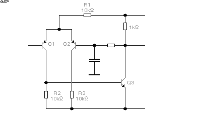
Figure 1a - Aesthetic
addition of resistor to balance the collector load.
As shown, and with a 12mA collector current for Q3, the load imbalance at the LTP is 202uA for Q1, and 915uA for Q2. Simply by reducing the value of R2, it is possible to improve matters, but it is still not going to give the performance of which the circuit is capable. Again, as shown the gain of the LTP is a rather dismal 66 (as measured at the collector of Q2).
Changing R1 for a current source does not help (gain is actually reduced slightly), but provides an improvement in power supply hum rejection and in particular improves common mode rejection. A common mode signal is one that is applied in the same phase and amplitude to both inputs at once.
The overall gain of this configuration (measured at the collector of Q3) is 590, but by reducing R2 to 1.8k, it can be raised to 910. This also improves collector current matching in the LTP, but the value will be device dependent, and is not reliable for production units..
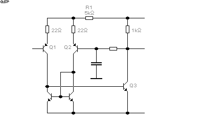
Figure 1b - A current
mirror and local feedback applied to the LTP
The circuit shown in Figure 1b has improved overall gain to 2010, a fairly dramatic improvement on the earlier attempt. A further improvement in linearity is to be had by adding resistors (100 Ohm or thereabouts) into the emitter circuits of the current mirror transistors. This will swamp the base-emitter non-linearities, and provide greater tolerance to device gain variations.
Proper selection of the operating current will improve matters considerably, and also help to reduce distortion, especially if local negative feedback (as shown in Figure 1b) is applied. This has been discussed at length by various writers [1], and a bit of simple logic reveals that benefits are bound to accrue to the designer who takes this seriously.
Since the value of the transistor's internal emitter resistance (re) is determined by the current flow -
At small currents (where the current variation during operation is comparatively high), this internal resistance has a pronounced effect on the performance of the stage. Simple solutions to apparently complex problems abound.
Use of a current mirror as the load for the long-tailed pair (LTP) again improves linearity and gain, allowing either more local feedback elsewhere, or more global feedback. Either of these will improve the performance of an amplifier, provided precautions are taken to ensure stability - i.e. freedom from oscillation at any frequency or amplitude, regardless of applied load impedance.
Single Transistor
There is another (not often used these days) version of an amplifier
input stage. This is a single transistor, with the feedback applied to
the emitter. It has been claimed by many that this is a grossly inferior
circuit, but it does have some very nice characteristics.
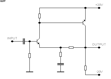
Figure 2a - Single Transistor
Input Stage
So what is so nice about this? In a word, stability. An amplifier using this input stage requires little or no additional stabilisation (the "Miller" cap, or "dominant pole") which is mandatory with amps having LTP input stages.
An amplifier using this input stage is referred to as a "current feedback" (CFB) circuit, since the feedback "node" (the emitter of the input transistor) is a very low impedance. The base circuit is the non-inverting input, and has a relatively high input impedance - but not generally as high as the differential pair. The +ve and -ve inputs are therefore asymmetrical. CFB amplifiers are used extensively in extremely fast linear ICs, and are capable of bandwidths in excess of 300MHz (that is not a misprint!).
This is the input stage used in the 10W Class-A amp (John Linsley-Hood's design, which is no longer a part of The Audio Pages), and also in the "El-Cheapo" amp described in my Projects Pages. "Well if it is so good, why doesn't anybody use it?" I hear you ask (you must have said it pretty loudly, then, because Australia is a long way away - from everywhere).
There is one basic limitation with this circuit, and this was "created" by the sudden requirement of all power amplifiers to be able to faithfully reproduce DC, lest they be disgraced by reviewers and spurned by buyers.
In addition, some form of biasing circuit is needed, and unfortunately this will either have to be made adjustable (which means a trimpot), or an opamp can be used to act as a DC "servo", comparing the output DC voltage with the zero volt reference and adjusting the input voltage to maintain 0V DC at the output. The use of such techniques will not be examined here, but can provide DC offsets far lower than can be achieved using the amplifier circuit itself. There is no sonic degradation caused by the opamp (assuming for the sake of the discussion that opamps cause sonic degradation anyway), since it operates at DC only (it might have some small influence at 0.5Hz or so, but this is unlikely to be audible).
It has also been claimed that the single transistor has a lower gain than the LTP, but this is simply untrue. Open loop gain of the stage is - if anything - higher than that of a simple LTP for the same device current.
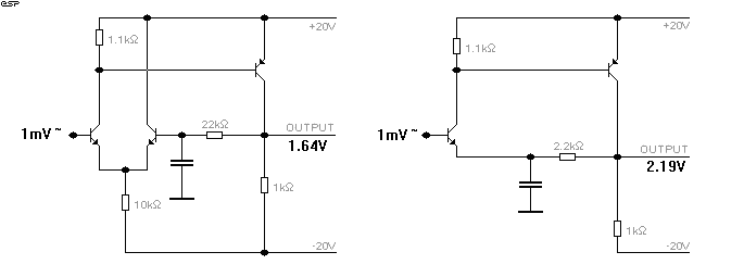
Figure 2b - Voltage Gain
Comparison Of Input Stages
I simulated a very simple pair of circuits (shown in Figure 2b) to see the difference between the two. Collector current is approximately 1mA in each, and the output of the LTP shows a voltage gain of 1,640 from the combined circuit (the input stage cannot properly be measured by itself, since it operates as a current amp in both cases). In neither case did I worry about DC offset, since the effects are minimal for the purpose of simply looking at the gain - therefore offset is not shown. (Did you notice that the gains obtained in this simulation are completly different from those obtained earlier for the simple LTP circuit - I used a different voltage (the previous example used +/- 12V). This in no way invalidates anything, they are just different.)
By comparison, the open-loop gain of the single transistor stage is 2,190 - considering that all other things were maintained equal, this is considerably better. Admittedly, the addition of a current mirror would improve the LTP even more dramatically, but do we really need that much more gain? A quick test indicates that we can get a gain of 3,570. This looks very impressive, but is only an increase of a little over 4.2dB compared to the single transistor. By the same logic, the single transistor only has a 2.5dB advantage over the simple LTP, however the difference may be moot ....
Because the single transistor stage requires no dominant pole Miller capacitor for stability, it will maintain the gain for a much wider frequency range, so in the long run might actually be far superior to the LTP. Further tests are obviously required (my simulator does not do distortion, so I'll have to build them).
Next Day ...
So I built them. Real life is never quite like the simulated version,
so there was a bit less gain from each circuit than the simulator claimed.
The LTP came in with an open loop gain of 1000, while the single transistor
managed 1400. The test conditions were a little different from the simulation,
in that +/-15 volts was used, so the gain difference is about what would
be expected, and is very close to the +/-12V results obtained in the first
set of simulations on the LTP.
Distortion was interesting, with the LTP producing 0.7% which was predominantly 3rd harmonic. The single transistor was slightly worse for the same output voltage with 0.9%, and this was mainly 2nd harmonic.
As expected, the LTP was unstable without a Miller capacitor, and 56pF managed to tame it down. Quite unexpectedly, the single transistor also required a Miller cap, but only when running open-loop. When it was allowed to have some feedback the oscillation disappeared. The LTP could not be operated without the Miller capacitor at any gain, and as the gain approached unity, more capacitance was needed to prevent oscillation.
The next step was a test of each circuit providing a gain of about 27, since this is around the "normal" figure for a 60W power amp. Here, the LTP is clearly superior, with a level of distortion I could not measure. The single transistor circuit had 0.04% distortion, and again this was predominantly 2nd harmonic. In this mode, no Miller capacitor was needed for the single transistor, and it showed a very wide frequency response, with a slight rise in gain at frequencies above 100kHz. This was also noticable with a 10kHz square wave, which had overshoot, although this was reasonably similar for positive and negative half-cycles. The LTP was well behaved, and showed no overshoot (it had the 56pF Miller cap installed), but it started to run out of gain at about 80kHz, and there was evidence of slew-rate limiting. This effect was not apparent with the single transistor.
All in all, I thought this was a worthwhile experiment, and the use of a simple resistor for the collector load of the gain stage allowed the final circuit to have a managable gain. Had a current source or similar been used as the load, I would not have been able to measure the gain accurately, since the input levels would have been too small. As it was, noise pickup proved to be a major problem, and it was difficult to get accurate results without using the signal averaging capability on the oscilloscope.
Conclusions
Based on the tests, there are pros and cons to both approaches - and
I bet that came as a surprise. The LTP in its simple form is a clear loser
for gain, but use of a current mirror allows it to "blow away" the single
transistor, which cannot capitalise on this technique since there is nothing
to mirror.
Stability is very important to me, and I tend towards an amp which absoultely does not oscillate, even at the expense of a little more distortion, but my own 60W reference amp is unconditionally stable with normal loads, and it uses an LTP for the input.
A favourite pastime of many designers is to connect a small capacitor as shown in Figure 3 directly to the base of the input transistor. This is supposed to prevent detection (rectification) of radio frequency signals picked up by the input leads. Well, to a certain degree this is true, as the Resistor-Capacitor (RC) combination forms a low pass filter, which will reduce the amount of RF applied to the input. As shown this has a 3dB frequency of 159kHz.
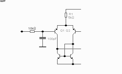
Figure 3 - The "traditional"
method for preventing RF detection.
Where things get really sneaky, is when the levels of RF energy are so high that some amount manages to get through anyway. I once had a workshop/lab which was "triangulated" by three TV transmission towers - very nasty.
The "traditional" method not only did not work, but made matters worse by ensuring that the transistor base was fed from a very low impedance (from an RF perspective). A vast number of commercial amplifiers and other equipment which I worked on in that time picked up quite unacceptable amounts of TV "frame buzz", caused by the detection of the 50Hz vertical synchronisation pulses in the TV signal. As the picture component of TV is amplitude modulated RF, this was readily converted into audio - of the most objectionable kind.
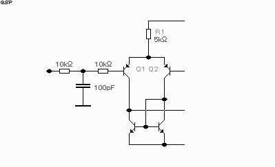
Figure 4 - Use of a "stopper"
resistor to prevent RF detection.
Figure 4 shows the remedy - but to be effective the resistor must be as close as possible to the base, or the performance is degraded. How does this work? Simple, the base-emitter junction of a transistor is a diode, and even when conducting it will retain non-linearities. These are often sufficient to enable the input stage to act as a crude AM detector, which will be quite effective with high-level TV or CB radio signals. Adding the external resistance again swamps the internal non-linearities, reducing the diode effect to negligible levels. This is not to say that it will entirely eliminate the problem where strong RF fields are present, but will at least reduce it to "nuisance" rather than "intolerable" levels.
UPDATE: I have been advised by a reader who works in a transmitting station that connecting the capacitor directly between base and emitter (in conjunction with the stopper resistor) is very effective. He too found that the traditional method was useless, but that when high strength fields are encountered, the simple stopper is not enough.
With opamps, the equivalent solution is to connect the stopper resistor in series with the +ve input, and the capacitor between the +ve and -ve inputs, with no connection to earth.
In all both cases it is essential to keep all leads and PCB tracks as
short as possible, so they cannot act as an antenna for the RF.
There are a number of traps here, not the least of which is that it is commonly assumed that the load (from the output stage) is infinite. Oh, sure, every designer knows that the Class-A stage must carry a current of at least 50% more than the output stage will draw, and this is easily calculated
For a typical 100W / 8 Ohm amplifier this will be somewhere between 5 and 10mA. Assuming an output transistor combination with a current gain of 1000 (50 for the driver, and 20 for the power transistor), with an 8 Ohm load, the impedance presented to the Class-A stage will be about 2k Ohms, which is a little shy of infinity.
Added to this is the fact that the impedance reflected back is non-linear, since the driver and output transistors change their gain with current - as do all real-life semiconductors. There are some devices available today which are far better than the average, but they are still not perfect in this respect.
The voltage gain is typically about 0.95 to 0.97 with the compound pair configuration. It must be noted that this figure will only be true for mid-range currents, and will be reduced at lower and higher values. Figure 5 shows the basic stage type - the same basic amplifier we used before, with the addition of a current source as the collector load. Also common is the "bootstrapped" circuit (not shown here).
There is not a lot of difference between current source and bootstrap circuits, but the current source has higher gain. With either type, there are some fairly simple additions which will improve linearity quite dramatically. Figure 5 shows the typical arrangement, but with the omission of the dominant pole stabilisation capacitor, which would normally be connected between the Class-A transistor's collector and base.
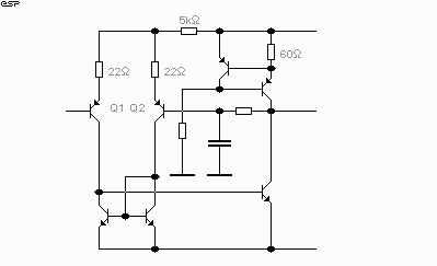
Figure 5 - Typical Class-A
driver configuration
It is therefore important to try to make the Class-A stage capable of high gain, even when loaded by the output stage. There have been many different methods used to achieve this, but none is completely successful. The biggest problem is that many designers seem completely oblivious to this problem area, or create such amazingly complex "solutions" as to make stabilisation almost impossible.
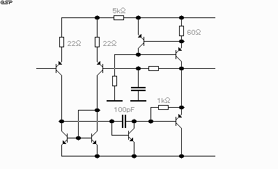
Figure 6 - One method
of improving the open loop output impedance of the Class-A driver.
The above is simple and very effective. This straightforward addition of an emitter follower to the Class-A driver (with the "bootstrap" resistor) has increased the combined LTP and Class-A driver gain to 1,800,000 (yes, 1.8 million!) or 125dB (open loop and without the dominant pole capacitor connected). Open loop output impedance is about 10k, again without the cap. Once the latter is in circuit, gain is reduced to a slightly more sensible 37,000 at 1kHz with the 100pF value shown. Output impedance at 1kHz is now - comparatively - very low, at about 150 Ohms.
Note that in the above, I have used a 5k resistor instead of the more usual current source. This is for clarity of the drawing, and not a suggestion that the current source should be forsaken in this position.
A special note for the unwary - If one is to use a single current control transistor for both the LTP and Class-A driver, do not use the Class-A current as the reference, but rather the LTP. If not, the varying current in the Class-A circuit will cause modulation of the LTP emitter current, with results that are sure to be as unwelcome as they are unpredictable [4].
I have often seen amplifier designs where the circuit is of such complexity that one must wonder how they ever managed to stop it from becoming high power radio frequency oscillators. The maze of low value capacitors sometimes used - some with series resistance - some without, truly makes one wonder what the open loop frequency and phase response must look like. Couple this with the fact that many of these amps do not have wonderful specifications anyway, and one is forced to ponder what the designer was actually trying to accomplish (being "different" is not a valid reason to publish or promote a circuit in my view, unless it offers some benefit otherwise unattainable).
UPDATE: Having carried out quite a few experiments over a period of a few weeks, I am not completely certain that vast amounts of gain from the input stage and Class-A amplifier stage are necessary. As long as the circuit is linear (i.e. has low distortion levels before the addition of feedback), the final result is likely to be satisfactory. I have seen many circuits with far more open loop gain than my reference amp (Project 03), and that in theory should be vastly superior - yet they are not.
There are essentially two ways to create a constant current "feed" to the Class-A driver stage. The active current source (as shown above) is one method, and this is very common. It does introduce additional active devices, but it is possible to make a current source that has an impedance so close to infinity that it will be almost impossible to measure it without affecting the result just by attaching measurement equipment. For more detailed information on current sources, see the article Current Sources Sinks and Mirrors.
A simpler way is to use the bootstrap circuit, where a capacitor is used from the output to maintain a relatively constant voltage across a resistor. If the voltage across a resistor is constant, then it follows that the current flowing through it must also be constant. Figure 6a (this was inserted after the other drawings were numbered) shows the circuit of a bootstrap constant current source. Unlike a true current source, the current through the bootstrap circuit will change with the supply voltage. This is a gradual change, and is outside the audio spectrum - or at least it should be if the circuit is designed correctly
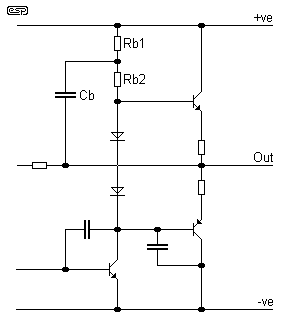
Figure 6a - Bootstrap
Current Source
This circuit works as follows. Under quiescent conditions, the output is at zero volts, and the positive supply is divided by Rb1 and Rb2. The base of the upper transistor will be at avout +0.7V - just sufficient to bias the transistor. As the output swings positive or negative, the voltage swing is coupled via Cb, so the voltage across Rb2 remains constant. The current through Rb2 is therefore constant, since it maintains an essentially constant voltage across it. Note that this applies only for AC voltages, as the capacitor will charge if there is a DC variation.
The overall difference is not great in a complete design. Although the current source is theoretically better, a bootstrap circuit is simpler and cheaper, and introduces no additional active devices.
There are countless amplifiers which still use the "darlington" type configuration, even though this was shown by many [2] to be inferior to the "complementary pair". Both configurations (in basic form, since there are many variations) are shown in Figure 7. There are two main areas where the darlington configuration is inferior, and we shall look at each ....
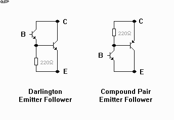
Figure 7 - The basic
configurations of output stages in common use.
Of the two shown, it will be apparent that I have ignored MOSFET output stages completely - this is by design, since I do not believe that they are really suitable for a serious hi-fi amplifier. As can be seen, the component count is the same for those shown, but instead of using two same polarity (both PNP or both NPN), the compound pair uses one device of each polarity. The final "device" assumes the characteristics of the driver in terms of polarity, and the Emitter, Base and Collector connections for each are shown. The resistor is added to prevent output transistor collector to base leakage current from allowing the device to turn itself on, and also speeds up the turn-off time. Omission of this resistor is not a common mistake to make, but it has been done. The results are degraded distortion - especially at high frequency - and poor thermal stability.
The value must be selected with reasonable care, if it is too low, the output transistor will not turn on under quiescent (no signal) conditions, and crossover distortion will result. If too high, turn-off performance will be impaired, and thermal stability will not be as good. The final value depends (to some extent) on the current in the Class-A driver stage and the gain of the driver transistor, but the final arbiter of quiescent is the Vbe multiplier stage.
Values of 100 Ohms - or as shown 220 Ohms should be fine for most amplifiers, with lower values used as power increases, which creates higher currents throughout the output stage and makes the transistors harder to turn off again, especially at high frequencies..
It can be seen that in the darlington configuration, there are two emitter-base junctions for each output device. Since each has its own thermal characteristic (a fall of about 2mV per degree C), the combination is notoriously difficult to make thermally stable. In addition, the gain of transistors often increases as they get hotter, thus compounding the problem. The bias "servo", typically a transistor "Vbe voltage multiplier, must be mounted on the heatsink to ensure good thermal equilibrium with the output devices, and in some cases can still barely manage to maintain thermal stability.
If stability is not maintained, the amplifier may be subject to "thermal runaway", where after a certain output device temperature is reached, the continued fall of Vbe causes even more quiescent current to flow, causing the temperature to rise further, and so on. A point is reached where the power dissipated is so high that the output transistors fail - often with catastrophic results to the remainder of the circuit and/or the attached loudspeakers.
The compound pair has only one controlling Vbe, and is thus far easier to stabilise. Since the single Vbe is that of the driver (which in many cases will not be mounted on the main heatsink, and in some will have no heatsink at all), the requirements for the Vbe multiplier are less stringent, mounting is far simpler and thermal stability is far better
I have used the compound pair for over 20 years, and when I saw it for the first time, it made too much sense in all respects to ignore. Thermal stability in a fairly basic 100W/4 Ohm amplifier of my design (of which hundreds were built) was assured with a simple 2-diode string - no adjustment was ever needed.
Numerous articles have been written on the superior linearity of the compound stage (Otala [3], Self, Linsley Hood among others) and I cannot help but be astonished when I see a new design in a magazine, still using the darlington arrangement. The use of the compound pair requires no more components - the same components are simply arranged in a different manner. It was with great gusto that an Australian electronics magazine recently proudly announced (in 1998) that "this is the first time we have used this arrangement in a published design" (or words to that effect).
What possible reason could they have had for not using the complementary
pair in every design they published (this magazine is a lot younger than
I). Words fail me. The magazine in question is not the only one, and the
Web abounds with designs old and new - all using the dreaded darlington
emitter-follower.
| Darlington | ||
| Driver | O/P Transistor | Total Gain |
| 50 | 25 | 1310 |
| Compound | ||
| Driver | O/P Transistor | Total Gain |
| 50 | 25 | 1290 |
The lower gain of the compound pair indicates that there is internal local negative feedback inherent in the configuration, and all tests that have been performed indicate that this is indeed true. Although the gain difference is not great, much of the improved linearity can be assumed to result from the fact that only one emitter-base junction is directly involved in the signal path rather than two, so only one set of direct non-linearities .is brought into the equation. The second (output) device effectively acts as a buffer for the driver.
Having said that, there are some very well respected amplifiers using darlington emitter-follower output stages. There are no hard and fast rules that can be applied to make the perfect amplifier (especially since it does not yet exist), and with careful design it is quite possible to make a very fine sounding amplifier using almost any topology.
It would seem (at first glance at least) that there is nothing to this piece of circuitry. It is a very basic Vbe multiplier circuit, and seemingly, nothing can go wrong. This is almost true, except for the following points.
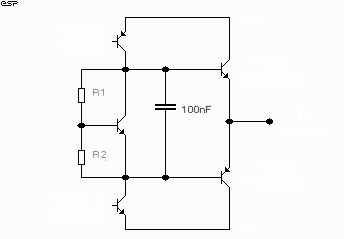
Figure 9 - The basic
bias servo circuit
The design of many amps (especially those using a darlington output stage) requires that the bias servo be made adjustable, to account for the differing characteristics of the transistors. If resistor R1 (in Fig 9) is instead a trimpot (i.e. variable resistor), what happens when (if) the wiper decides (through age, contamination or rough handling) to go open-circuit?
The answer is simple - the voltage across the bias servo is now the full supply voltage (less a transistor drop or two), causing both the positive and negative output devices to turn on as hard as they possibly can. The result of this is the instantaneous destruction of the output devices - this will happen so fast that fuses cannot possibly prevent it, and even the inclusion of sophisticated Load-Line output protection circuitry is unlikely to be able to save the day.
The answer of course is so simple that it should be immediately obvious to all, but sadly this is not always the case. By making R2 the variable component, should it happen to become open-circuited the bias servo simply removes the bias. This will introduce crossover distortion, but the devices are saved. To prevent the possibility of reducing the pot value to 0 ohms (which will have the same effect as described above!), there should be a series resistor, whose value is selected to allow adequate adjustment while retaining a respectable safety margin.
An additional precaution must be taken here, in that if the resistor values are too low, the offset voltage seen by the output transistors is simply the voltage drop across the resistors, with the transistor having little or no control over the result. This is easily avoided by ensuring that the resistor current is 1/10 (or thereabouts) of the total Class-A bias current.
UPDATE: It is also quite possible to make the resistance too large, so the bias servo will amplify the temperature change too much. This will cause the amplifier's quiescent current to fall as it gets hotter. While this is a good thing from the reliability point of view, if it causes crossover distortion to appear when the amp is hot, the audible effect will obviously be a disaster. It will generally be necessary to experiment with the values to ensure that stability is maintained - there is no way to calculate this that comes to mind, although I am sure it is possible. The base-emitter voltage falls at 2mV / degree C, but the variation in gain with temperature is not as readily calculated.
As a secondary safeguard, using a suitable diode string in parallel with the servo is suggested. These should be chosen to prevent destructive current, but some method of overtemperature protection will be needed.
It is a simple fact of life that an emitter follower (whether darlington or compound) is perfectly happy to become an oscillator - generally at very high frequencies. This is especially true when the output lead looks like a tuned circuit. A length of speaker cable, while quite innocuous at audio frequencies, is a transmission line at some frequency determined by its length, conductor diameter and conductor spacing. A copy of the ARRL handbook (from any year) will provide all the formulae needed to calculate this, if you really want to go that far.
All power amplifiers (well, nearly all) use emitter follower type output stages, and when a speaker lead and speaker (or even a non-inductive dummy load) are connected, oscillation often results. This is nearly always when the amp is driven, and is more likely when current is being drawn from the circuit. It is a little sad that the compound pair is actually more prone to this errant behaviour than a darlington, possibly because the driver is the controlling element (and its emitter is connected to the load), and has a higher bandwidth.
Some of the "super" cables - much beloved by audiophiles - are often worse in this respect for their ability to act as RF transmission lines than "ordinary" Figure-8 or 3-core mains flex, and are therefore more likely to cause this problem.
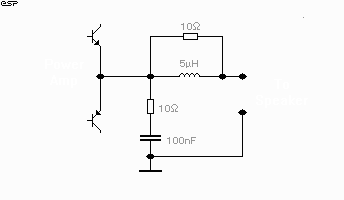
Figure 10 - The standard
output arrangement for power amp stability.
The conventional "Zobel" network (consisting of the 10 Ohm resistor and 100nF capacitor) generally swamps the external transmission line effect of the speaker cables and internal wiring, and provides stability under most normal operating conditions.
With capacitive loading (as will be the case when a loudspeaker and passive crossover are connected), the Zobel network has no additional effect whatsoever. The only sure way to prevent oscillation or severe ringing is to include an inductor in the output of the amplifier. This should be bypassed with a suitable resistor to reduce the Q of the inductor, and the typical arrangement is shown in Fig 10. For readers wishing to explore this in greater depth, read "The Audio Power Interface" [2]. Of late (see the note below), I have been suitably perplexed by the sudden appearance of distortion in an amp, simply by adding the inductor. On the basis of this, it might be better to use a far lower resistance than the 10 Ohms specified above - I am thinking 1 Ohm or maybe even less !
Another alternative is to include a resistor in series with the output of the amplifier, but this will naturally have the dual effect of reducing power output and reducing damping factor. At resistor values sufficient to prevent oscillation, the above losses become excessive - and all wasted power must be converted into heat in the resistor.
The choice of inductor size is not difficult - for an 8 Ohm load it will be typically a maximum of 6uH, any larger than this will cause unacceptable attenuation of high frequencies. A 6uH inductor as shown in Figure 10 will introduce a low frequency loss (assuming 0.03 Ohm resistance) of 0.03dB. and will be about 0.2dB down at 20kHz. These losses are insignificant, and will not be audible. In contrast, ringing (or in extreme cases, oscillation) of the output devices will be audible (even at very low levels) as increased distortion, and in extreme cases may destroy the transistors.
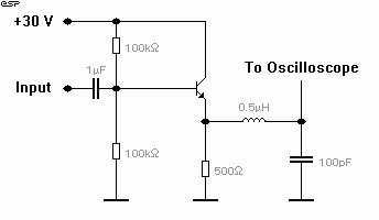
Figure 11 - Lumped component
transmission line causes emitter follower to oscillate.
In simulations and on the lab bench, I have been able to make a single transistor emitter follower circuit oscillate quite happily, with a real transmission line (such as a length of co-axial cable), or a lumped component equivalent of a transmission line, consisting of a 5nH inductor and 100pF as a series tuned circuit. This is shown in Figure 11.
Figure 12 - Simulator
oscilloscope display of oscillation in emitter follower
This effect is made worse as the source impedance is lowered, but even a base "stopper" resistor will not prevent oscillation - only the swamping effect of the transmission line by a Zobel network succeeds. In case you were wondering why the oscilloscope "take-off" point is at the junction of the L and C components, this allows series resonance to "amplify" the HF component, making it more readily seen.
In my own amp (the one that hundreds of were made), I did not use an output inductor, but instead made the dominant pole (the capacitance from the collector to base of the Class-A driver) somewhat larger than normal. This managed to keep the amp stable under all operating conditions, but at the expense of slew rate (and consequent slew rate limited power at high frequencies). This was largely an economic decision, since a couple of ceramic capacitors are much cheaper than an inductor, and the amp was used largely for musical instrument amplification so an extended high frequency response was actually undesirable. Full power bandwidth - the ability of an amp to supply full power over its entire operating frequency range - is a sure way to destroy hearing, HF horn drivers (etc) in a live music situation, so the compromise was not a limitation. However .
There is another reason that a series output inductor may be helpful. It has been suggested (but by whom I cannot remember) that radio frequencies picked up by the speaker leads may be injected back into the input stage via the negative feedback path. When one looks at a typical circuit, this seems plausible, but I have not tested the theory too deeply.
The basics behind it are not too difficult to work out, however. Since it is known that there must be a dominant pole in the amplifier's open-loop frequency response (the capacitor shown in Figures 5 and 6) if it is to remain stable when feedback is applied, it follows that as internal gain decreases with increasing frequency then the output impedance must rise (due to less global feedback). Indeed this is the case, and by the time the frequency is into the MHz regions, there will be negligible loading of any such frequencies by the output stage.
If appropriate precautions are not taken (as in Figure 4) for the negative
feedback return path, then it is entirely likely that RF detection could
occur. In my own bi-amped system (which uses the amplifier described above,
still without an output inductor), I recently had problems with detection
of a local AM radio station. Fitting of RF "EMI" suppression chokes (basically,
loop the speaker cable through a ferrite ring 3 or 4 times) completely
eliminated the problem, so I must conclude that it is indeed possible or
even probable.
It is doubtful that my amplifier is the only design to exhibit this behaviour, so it must be said that some amps may not be happy with an output inductor. It is not possible to predict that combination of circumstance that will cause a problem, one more reason that design of amplifiers is fraught with danger if proper testing facilities are not available.
The maximum output current of a power amplifier is often thought to be something that affects the output transistors only, and that adding more transistors will automatically provide more current to drive lower impedances. This is only partially true, because bipolar transistors need base current, and this must come from the driver stage.
It is common to bias the Class-A driver stage so that it can provide between 1.5 to 5 times the expected base current needed by the output transistors. As the current in this stage is lowered, there is likely to be a substantial increase in the distortion, since the current will change by a larger percentage. If the Class-A driver current is too high, there will be too much heat to get rid of, and it is possible to exceed the transistor's maximum ratings. I normally work to a figure of about double the expected output device base current, but in some cases it will be less than this.
As an example, let's look at a typical power amplifier output stage. Assuming a power supply of +/-35V, the maximum output current will be 35 / 8 = 4.375 Amps (an 8 ohm load is assumed). Since we know that there will be some losses in the driver / power transistor combination, we can safely assume a maximum current of 4A. A suitable power transistor may be specified for a minimum gain (Hfe) of 25, with a collector current of 4A. The driver transistors will generally have a higher gain - perhaps 50 at a collector current of 250mA. The product of the two current gains is accurate enough for what we need, and this gives a combined Hfe of 1,000. The peak base current will therefore be 4mA.
If we choose to use a Class-A driver current of double the expected output device base current, this means that the driver will operate at about 8mA. This could be achieved with a current source, or a bootstrapped circuit using a pair of 2.2k resistors in series. At the maximum voltage swing (close to +/-35V), the driver current will be increased to 12mA or decreased to 4mA, depending on the polarity. The current source or bootstrap circuit will maintain a constant current, but the driver has to deal with a current that varies by +/-4mA as the current into the load changes.
If the load impedance is dropped to 4 ohms, the current source will still only be able to provide 8mA, so output current will be limited to 8A - the driver at this point in the cycle has zero current. At the opposite extreme, the driver will have to cope with 16mA when it is turned on fully. At lower impedances, the driver will be able to supply more current, but the current source will steadfastly refuse to provide more than the 8mA it was designed for, so the peak output current will be limited to 8A in one direction (when the current source provides the drive signal and the Class-A driver is turned off), or some other (possibly destructive) maximum current in the opposite polarity.
But hang on! A Class-A driver is called a Class-A driver because it never turns off - we now have a Class-AB driver, which is not the desired objective! The amplifier will clip asymmetrically, and is no longer operating in the linear range - it is distorting.
Adding more power transistors will provide a very limited benefit, since the maximum base current is still limited by the current source supplying the Class-A driver. In order to obtain maximum power at lower impedances requires that either the gain of the output stage is increased, or the Class-A driver current must be increased. Increasing the gain of the output stage devices is not trivial - you must either use a different topology or higher gain power and driver transistors.
The design phase of an amplifier follows similar guidelines, regardless of topology. From Amplifier Basics ...
For the sake of simplicity, if bipolar output transistors have a gain
of 20 at the maximum current into the load, the drivers must be able to
supply enough base current to allow this. If the maximum current
is 4A, then the drivers must be able to supply 200mA of base current to
the output devices.
Again, using the bipolar example from above, the maximum base current
for the output transistors was 200mA. If the drivers have a minimum
specified gain of 50, then their base current will be
200 / 50 = 4mA.
Since the Class-A driver must operate in Class-A (what a surprise),
it will need to operate with a current of 1.5 to 5 times the expected maximum
driver current, to ensure that it never turns off. The same applies
with a MOSFET amp that will expect (for example) a maximum gate capacitance
charge (or discharge) current of 4mA at the highest amplitudes and frequencies.
Information added 09 Jun
2001
When specified, regulation is based upon a resistive load over the full cycle, but when used in a capacitor input filter (99.9% of all amplifier power supplies), the quoted and measured figures will never match.
Since the applied AC spends so much of its time at a voltage lower than that of the capacitor, there is no diode conduction. During the brief periods when the diode conducts, the transformer has to replace all energy drained from the capacitor in the intervening 7 to 8ms or so (assuming 50Hz and full wave rectification).
Consider a power supply as shown in Figure 13. This is a completely conventional full-wave capacitor input filter (it is shown as single polarity for convenience). The circuit is assumed to have a total effective series resistance of 1 Ohm - this includes transformer winding resistances (primary and secondary) and diode losses. The capacitor C1 has an initial value of 4,700uF.
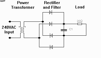
Figure 13 - Full Wave,
Capacitor Input Filter Rectifier
The transformer is rated at 60VA and has a primary resistance of 15 Ohms, and a secondary resistance of 0.5 Ohms. This calculates to an internal "copper loss" of 0.75 Ohm.
With a 20 Ohm load as shown, and at an output current of about 1.7 amps (1.69A actually), diode conduction is about 2.8ms, and the peak value of the current flowing into the capacitor is 6A - 100 times per second (10ms interval). Diode conduction is therefore 28% of the cycle. (To check that these figures are valid, we can take the peak capacitor current and the duty cycle, and calculate the average
For this example, this works out to 17.5% which is terrible. By comparison, the actual transformer regulation would be in the order of 5% for a load current of 2A at 30V. Note that the RMS current in the secondary of the transformer will be 2A AC (i.e. DC current by root two), for a load current of 1.7A DC - this must be so, since otherwise we would be getting something for nothing - a practice frowned upon by physics and the taxman.
Output power is 33.8V * 1.7A = 57.46W, and input power is 240V * 0.25A
= 60W (VA actually, but we won't split hairs here). The losses are caused
by the diode voltage drop and winding resistance of the transformer.
| Capacitor Ripple Current - It is well known that bigger transformers
have better efficiency that small ones, so it is a common practice to use
a transformer that is over-rated for the application. This can improve
the regulation considerably, but also places greater stresses on the filter
capacitor due to higher ripple current. This is quoted in manufacturer
data for capacitors intended for use in power supplies, and must not be
exceeded. Excessive ripple current will cause overheating and eventual
failure of the capacitor.
Large capacitors usually have a higher ripple current current rating than small ones (both physical size and capacitance). It is useful to know that two 4,700uF caps will usually have a higher combined ripple current than a single 10,000uF cap, and will also show a lower ESR (equivalent series resistance). The combination will generally be cheaper as well - one of the very few instances where you really can get something for nothing. |
For further reading on this topic, see the Linear Power Supply Design article
If I never hear of someone complaining that "distortion measurements are invalid, and a waste of time" again, it will be too soon. I am so fed up with so-called experts (where "x" is an unknown quantity, and a "spurt" is a drip under pressure) claiming that "real world" signals are so much more complicated than a sinewave, and that static distortion measurements are completely meaningless.
They are not meaningless, and real world signals are sinewaves! The only difference is that with music, there is usually a large number of sinewaves, all added together. There is not a myriad of simultaneous signals passing through an amp, just one (for a single channel, naturally).
Since physics tells us that no two masses can occupy the same physical space at the same time, so it is with voltages and currents. There can only ever be one value of voltage and one value of current flowing through a single circuit element at any instant of time - if it were any different, the concept of digital recording could never exist, since in a digital recording the instantaneous voltage is sampled and digitised at the sampling rate. This would clearly be impossible if there were say 3 different voltages all present simultaneously.
So, how do these x-spurts determine if an amplifier has a tiny bit of crossover distortion (for example). I can see it as the residual from my distortion meter, and it is instantly recognisable for what it really is, and I can see the difference when I make a change to a circuit to eliminate the problem. If I had to rely on my ears (which although getting older, still work quite well), It would take me much longer to identify the problem, and even longer to be certain that it was gone. I'm not talking about the really gross crossover distortion that one gets from an under-biased amp, I am referring to vestiges - miniscule amounts that will barely register on the meter - I use my oscilloscope to see the exact distortion waveform. I suspect that this dilemma is "solved" by some by simply not using the push-pull arrangement at all, thereby ensuring that power is severly limited, and other distortion is so high that they would not dare to publish the results.
These same x-spurts will wax lyrical about some really grotty single ended triode amp, with no power and a highly questionable output transformer, limited frequency response and a damping factor of unity if it is lucky.
Don't get me wrong - I'm not saying that this is a definition of single-ended triode amps (for example), there are some which I am sure sound very nice - not my cup of tea, but "nice". I have seen circuits published on the web that I would not use to drive a clock radio speaker (no names, so don't ask), and "testimonials" from people who have purchased this rubbish, but there are undoubtedly some that do use quality components and probably sound excellent at low volume levels.
Sorry if I sound vehement (vitriolic, even), but quite frankly this p****s me off badly. There are so many people waving their "knowledge" about, and many of them are either pandering to the "Magic Market", or talking through their hats.
The whole idea of taking measurements is to ensure that the product meets some quality standard. Once this standard is removed, and we are expected to "let our ears be the judge", how are we supposed to know if we got what we paid for? If the amp turns out to sound revolting (to us), should we accept this, or perhaps we should listen to it for long enough that we get used to the sound (this will happen - eventually). I am not willing to accept this, and I'm sure that many others feel the same.
Please don't think that I am advocating "specsmanship", because I'm not. I just happen to think that consumers are entitled to some minimum performance standard that the equipment should meet (or exceed). I have yet to hear any amplifier with high distortion levels and/or limited bandwidth sound better than a similar amplifier with lower distortion and wider bandwidth. This implies that we compare like with like - a comparison between a nice valve amp and a nasty transistor amp will still show the transistor amp as having better specs, but we can be assured that it will sound worse.
This is an argument that has been going for years, and it seems we are no closer to resolving the dilemma than we ever were. I have worked with all three, and each has its own sonic quality. Briefly, we shall have a look at the differences - this is not an exhaustive list, nor is it meant to be - these are the main points, influenced by my own experiences (and I must admit, prejudices). Please excuse the somewhat random order of the comparisons :
Valves :
Valves are Voltage to Current Converters, so the output current is
controlled by an input voltage. It is necessary to apply the varying
output current to a load (the anode resistor or transformer) to derive
an output voltage.
There is no such thing at the time of writing as the much sought after (but elusive) "straight wire with gain". But wait - there's more ....
Another aspect of amplifier design is slew rate. This term is not well understood, and the possible effects even less so.
Slew Rate Nomograph
It has been claimed by many writers on the subject that a "slew-rate
limited" amplifier will introduce transient intermodulation distortion,
or TIM. In theory, this is perfectly true, provided that the slew
rate is sufficiently low as to be within the audible spectrum (i.e. below
20 kHz), and the program material has sufficient power at such high frequencies
to cause the amplifier to limit in this fashion.
The following nomogram is helpful in allowing you to determine the required slew rate of any amplifier, so that it can reproduce the required audio bandwidth without introducing distortion components as a result of not being fast enough.
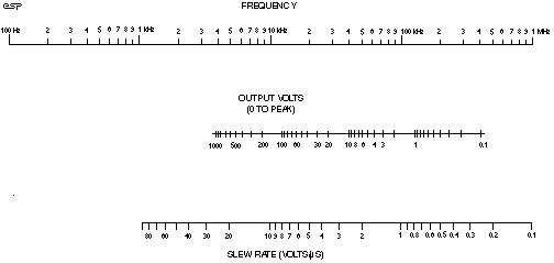
Figure 14 - Slew Rate
Nomograph
To use this nomograph, first select the maximum frequency on the top row. Let's assume 30kHz as an example. Next, select the actual output voltage (peak, which is RMS * 1.414) that the amplifier must be able to reproduce. For a 100W 8 Ohms amp, this is 28V RMS, or 40V peak. Now draw a line through these two points, and read the slew rate off the bottom row. For the example, this is 8V/us. This is in fact far in excess of what is really needed, since it is not possible for an amp reproducing music to have full power at 30kHz
By 20kHz, our 100W amp will need a maximum of 10W (typically much less), and this is only about 12V peak. Using the nomograph with this data reveals that a slew rate of about 2V/us is quite sufficient. Such an amp will go into what is known as "slew rate limiting" at full power with frequencies above 10kHz or so, converting the input sinewave into a triangular wave whose amplitude decreases with increasing frequency.
Some claim that this is audible, although this is purely subjective. That a typical audio signal is a complex mixture of signals is of no real consequence, because an amp has no inherent concept of "complex" any more than it has an opinion about the date. At any given point in time, there is an instantaneous value of input voltage that must be increased in amplitude and current to drive the loudspeaker. As long as this input voltage does not change faster than the amplifier is capable of doing, then no degradation is should occur.
Although this is a fine theory, there seems to be too much entrenched prejudice against "slow" amplifiers, which may indeed sound different from another that is not constrained by slew rate limiting - at least within the full audible range.
As shown above, the slew rate of an amplifier is usually measured in Volts / microsecond, and is a measure of how fast the amplifier's output can respond to a rapidly changing input signal. Few manufacturers specify slew rate these days (mainly because few buyers understand what it is), but it is an important aspect of an amplifier's design.
As can be seen from the above, for an amplifier (of any configuration) to reproduce 28V at 20 kHz (about 100W / 8 Ohms) requires a slew rate of 4.4 V / us. This is to say that the output voltage can change (in any direction) at the rate of 4.4 Volts in one microsecond. This is not especially fast, and as should be obvious, is dependent upon output voltage. A low power amp need not slew as fast as a higher powered amp. There is no real requirement for any amp to be able to slew faster than this, as there is a significantly large margin provided already. This can be calculated or measured - I measured it at 22V maximum rate of change in 5us (give or take a little), which works out to 4.4V/us again.
Doubling the amplifier's output voltage (four times the power) requires that the slew rate doubles, and vice versa, so a 400W amp needs a slew rate of 8.8 V / us, while a 25W amp only needs 2.2 V /us. This is a very good reason to use a smaller amplifier for tweeters in a tri-amped system, since it is much easier to achieve a respectable slew rate when vast numbers of output devices are not required.
Essentially, if the amplifier's output cannot respond to the rapidly changing input signal, an error voltage is developed at the long-tailed pair stage, which tries to correct the error. The LTP is an amplifier, but more importantly, an error amplifier, whose sole purpose is to keep both of its inputs at the same voltage. This is critical to the operation of a solid state amp, and the LTP output will generally be a very distorted voltage and current waveform, producing a signal that is the exact opposite of all the accumulated distortions within the remainder of the amp (this also applies to opamps).
The result is (or is supposed to be) that the signal applied to the inverting input is an inverted exact replica of the input signal. Were this to be achieved in practice, the amp would have no distortion at all. In reality, there is always some small difference, and if the Class-A driver or some other stage enters (or approaches) the slew rate limited region of operation, the error amp (LTP) can no longer compensate for the error.
Once this happens distortion rises, but more importantly, the input signal is exceeding the capabilities of the amplifier, and the intermodulation products rise dramatically. Intermodulation distortion is characterised by the fact that a low frequency signal modulates the amplitude (and / or shape) of a higher frequency signal, generating additional frequencies that were not present in the original signal. This also occurs when an amplifier clips, or if it has measurable crossover distortion.
Sounds like ordinary distortion, doesn't it? That too creates frequencies that were not in the original, but the difference is that harmonic distortion creates harmonics (hence the name), whereas intermodulation distortion creates frequencies that have no harmonic relationship to either of the original frequencies. Rather, the new frequencies are the sum and difference of the original two frequencies. (This effect is used extensively in radio, to create the intermediate frequency from which the audio, video or other wanted signal can be extracted.) The term "harmonic" basically can be translated to "musical", and "non-harmonic" is mathematically derived, but not musically related .... if you see what I mean.
Whenever the LTP loses control of the signal, intermodulation products will be generated, so the bandwidth of an amplifier must be wide enough to ensure that this cannot happen with any normal audio input signal. There is nothing wrong or difficult about this approach, and it is quite realisable in any modern design. Although unrealistic from a musical point of view, it is better if an amplifier is capable of reproducing full power at the maximum audible frequency (20 kHz) than if it starts to go into slew rate limiting at some lower frequency.
The reason I say it is unrealistic musically is simply because there is no known instrument - other than a badly set up synthesister - that is capable of producing any full power harmonic at 20 kHz, so in theory, the amp does not have to be able to reproduce this. In reality, inability to reproduce full power at 20 kHz means that the amp will very likely suffer from some degree of transient intermodulation distortion with some program material.
This is not a problem that affects simple amps with little or no feedback - they generate enough harmonic distortion to more than make up for the failings of more complex circuits, with lots of global feedback. This fact tends to annoy the minimalists, who are often great believers in no feedback under any circumstance, which relegates them to listening to equipment that would have been considered inferior in the 1950's.
Few sensible people would argue that measurements of frequency response are unimportant or irrelevant, and this is one of the simplest measurements to take on an amplifier. Again, the subjectivists would have it that these fail to take into account some mysterious area of our brain that will compensate for a restricted response, and allow us to just enjoy the experience of the sound system. This is true - we will compensate for diminished (or deranged) frequency response, but it need not be so.
If you listen to a clock radio for long enough, your brain will think that this is normal, and will adjust itself accordingly. Imagine your surprise when you hear something that actually has real low and high frequencies to offer - the first reaction is that there is too much of everything, but again, the brain will make the required allowances and this will sound normal after a time.
There are so many standard measurements on amplifiers that are essential to allow us to make an informed judgement (is this amp even worth listening to?). I really object to the attitude that "it does not matter what the measurements say, it sounds great". In reality this is rarely the case - if it measures as disgusting, then it will almost invariably sound disgusting. There is no place for hi-fi equipment that simply does not meet some basic standards - and I have never heard an amp that looked awful on the oscilloscope, measured as awful on my distortion meter, but sounded good - period.
For further reading, I strongly recommend "The Self Site", and in particular "Science and Subjectivism in Audio" and also my own article on the subject "Cables, Interconnects & Other Stuff - The Truth". There is also a new article (as of 26 Feb 2000) called "Amplifier Sound - What Are The Influences?" that goes a little deeper into the measured and subjective performance of amplifiers, and suggests a couple of new tests that might be applied.